TBC: The Tiny Binary Computer
"Greyed out" material in the documentation describes features that are planned but not yet implemented.
To write and run programs for TBC, you only need to read Introduction, Assembler and Instruction Set, and Operation. If you want to know more about how a small computer like this one could be realized in hardware and how close the simulation comes to such a realization, you will find that information in Architecture and Micro-Architecture.
Table of Contents
Introduction
TBC, the Tiny Binary Computer is a language translator and simulator for a computer with a very limited instruction set and very limited memory. Even so, you can write and run interesting programs with it. The assembler is TBC's language translator. It translates human-readable source programs into binary machine instructions for the virtual machine. The virtual machine is a simulation of the computer. It can load and run programs that have been translated by the assembler.
To write programs for TBC, you will need to read the section Assembler and Instruction Set. To run your programs after they've been translated, you will need to read the Operation section. The Architecture and Micro-Architecture section describes the technical details of the simulated computer that is TBC. With the exception of the input and output facility, there is enough information to construct a prototype from digital logic.
You will find programming to be much easier if you express your algorithms in pseudo code before you begin writing TBC instructions. That allows you to separate the process of algorithm development from the process of programming. That is especially important if you are writing in an assembler language.
Assembler and Instruction Set
The TBC assembler has two panes. The left pane is the source code pane; a source program in the format described below can be loaded from the browser's local storage, pasted into the pane from an external editor, or created by typing directly into the pane. (Note: in web browsers, the tab key moves focus from item to item, and so cannot be used to enter tab characters into the pane.)
A source program loaded from local storage can (and should!) be saved with the "Save" button if it has been modified. An new program should be given a file name with the "Save as" button and input area. File names are limited to upper- and lower-case letters plus digits and underscore. File names are case sensitive.
The "Assemble" button translates the source code into TBC binary object code and produces a listing in the right pane. If there were no assembly errors, the object code is also saved in local storage using the same base name as the source file. A source program that has not been given a name by saving it with "Save as" cannot be assembled.
The "Print" button prints the result of the assembly process.
The file selector and "Delete" button at the far right of the button area allows files saved in local storage to be deleted. The source file and object file (if it exists) are deleted. Deleted files cannot be recovered.
For security reasons, web programs cannot write disk files directly. To save a file outside TBC, load it into the assembler's left pane and use copy-and-paste to copy it to an editor.
Format of Assembly Language Statements
Assembly language statements for TBC are of the form:
The label, if present, must begin at the left, with no preceding white space. The operation code must be preceded by white space regardless of whether a label is present. (This is different from LMC, which allows operation codes to begin at the left.)
Labels, operation codes, and symbolic addresses are case-insensitive. Labels and symbolic addresses are not length-limited. For valid operation codes, see Instruction Set, below.
Addresses may be symbolic addresses, which correspond to labels defined elsewhere in the source program, or numeric addresses. Numeric addresses may be expressed as decimal numbers or hexadecimal numbers. Hexadecimal numbers must be prefixed with "0x" –the digit zero followed by the letter x. Example: 0x5A or 0x5a. Addresses are limited to the range 0-127 or 0x0 to 0x7f.
Anything following the address, or for operation codes that do not take an address, anything following the operation code, is treated as a comment.
By default the assembler generates object code beginning at location zero. The address where a sequence of instructions will be loaded can be changed using the org assembler directive, which takes a numeric address as an operand. Example:
             org      0x50
             add      const1      The "add" instruction will be at address 0x50
             brp      done        BRP will be at 0x51, etc.
    const1   dat      1           A data value
The first executable instruction must be at location zero, as it will be by default.
For information about defining data, see The Secrets of dat below.
Instruction Set
TBC's instruction set is a superset of that of Stuart Madnick's Little Man Computer, and with the same semantics. In the table below, <addr> represents a numeric or symbolic address, xx represents the address as two hexadecimal digits, and <str> represents a character string. The synonyms for operation codes accommodate different "dialects" of LMC.
| Mnemonic | Op code | Description |
|---|---|---|
| ADD <addr> | 1xx | Add. The contents of memory at address <addr> are added to the accumulator. An Overflow machine-check occurs if the result is greater than 2047 or less than -2048; the truncated result is stored in the accumulator. |
| SUB <addr> | 2xx | Subtract. The contents of memory at address <addr> are subtracted from the accumulator. An Overflow machine-check occurs if the result is greater than 2047 or less than -2048; the truncated result is stored in the accumulator. |
| STA <addr> | 3xx | Store accumulator. The contents of the accumulator are stored in memory at address <addr>; the previous contents of memory at <addr> are lost. The mnemonic STO is accepted as a synonym for STA. |
| LDA <addr> | 5xx | Load accumulator. The contents of memory at address <addr> are loaded into the accumulator; the previous contents of the accumulator are lost. |
| BR <addr> | 6xx | Branch unconditionally. The value of <addr> is stored in the program counter, causing the next instruction to be fetched from that location. The mnemonic BRA is accepted as a synonym for BR. |
| BRZ <addr> | 7xx | Branch if zero. If the accumulator holds the value zero, the value of <addr> is stored in the program counter, causing the next instruction to be fetched from that location. If the accumulator is non-zero, the program counter is not modified and the next instruction will be fetched in sequence. The accumulator is not modified. |
| BRP <addr> | 8xx | Branch if positive. If the sign bit of the accumulator is zero, the value of <addr> is stored in the program counter, causing the next instruction to be fetched from that location. If the sign bit is one, the program counter is not modified and the next instruction will be fetched in sequence. The accumulator is not modified. Note that a value of zero in the accumulator will cause the branch to be taken because the sign bit of the number zero is zero. |
| IN | 901 | Input. A number is requested from the input subsystem and stored in the accumulator. The previous contents of the accumulator are lost. The input subsystem will not deliver values greater than 2047 nor less than -2048. The mnemonic INP is accepted as a synonym for IN. |
| OUT | 902 | Output. The contents of the accumulator are copied to the output subsystem as a decimal value, followed by the newline character. The accumulator is not changed. |
| DAT | Data. Reserves and optionally initializes one word of data. If a numeric operand in range -2048..2047 is given, the storage word is initialized to the operand value. | |
| HLT | 0xx | Halt. Instruction execution stops. Operating the "reset" switch will restart the program from location zero. The mnemonic COB is accepted as a synonym for HLT. |
Extended Instructions (Not part of the LMC instruction set)
| CALL <addr> | Axx | Subprogram call. The number at the highest memory address is decremented, the program counter is stored at the address pointed by the contents of the highest memory address, and the <addr> portion of the instruction is placed in the program counter. In other words, the highest memory address is used as a stack pointer for a stack that grows downward from high memory. Resetting the machine or loading a program stores the address of the highest memory location in that location. For a machine with 128 words of storage, the value 0x7F is stored at location 0x7F. |
| RET | F04 | Return from subprogram. The memory location pointed by the contents of the highest memory address is loaded into the program counter and the value at the highest memory address is decremented. Only the rightmost eight bits of the value on the stack are used. |
| CMPL | F01 | Complement. The twos complement of the contents of the accumulator is loaded into the accumulator. |
| DAT "<str>" | Character data pseudo-instruction. The characters in <str>, which must be enclosed in double-quotes, are stored in the rightmost eight bits of consecutive words. Example: DAT "Hello, world!" Strings must not extend across lines. Escaped characters are not allowed. A newline character may be stored by coding DAT 0x00A. If 0x00A is processed by an OUT instruction, it will be rendered as 10. If it is processed by OUTC, it will be rendered as newline. |
|
| DAT <list> | Multiple data pseudo-instruction. A list of decimal or hexadecimal numbers separated by commas, are stored in consecutive words. Example: DAT "Hello",0x0A,0 Lists must not extend across lines. End of line or the first space character terminates the list. |
|
| INC | F02 | Increment. The contents of the accumulator are incremented and the result is loaded into the accumulator. |
| LIA | F03 | Load Indirect Accumulator. Performs a load using the contents of the accumulator as the address. Warning: Because the accumulator can contain values greater than the highest installed memory address, a programming error can cause a "Machine check; memory reference error." |
| LDI <const> | 4xx | Load Immediate. The the address field of the instruction is loaded into the accumulator as a positive number in range 0..255. Note: If a symbol is given as an operand, the value (address) of the symbol is loaded. |
| ORG | Set origin pseudo-instruction Sets the address at which successive instructions or data will be stored. For example, instructions or data following: ORG 0x50 will be stored beginning at address 0x50. The operand may be decimal or hexadecimal. The asterisk character * is accepted as a synonym for ORG. | |
| OUTC | 904 | Output character. The rightmost eight bits of the accumulator are sent to the output subsystem, to be interpreted as an ISO-8859 character rather than a number. No newline character is sent. See "DAT <str>" for information about sending a newline. |
| OUTN | 903 | Output with No newline. Identical to OUT except that sending the newline character is suppressed. |
| PUSH | F05 | Push value onto stack. The contents of the accumulator are stored at the location pointed by the stack pointer and the stack pointer is decremented. (The stack grows downward and the stack pointer points to the first empty stack frame.) |
| POP | F06 | Pop value from stack. The stack pointer is incremented and the accumulator is loaded from the address in the stack pointer. (The stack grown downward.) |
| SSWP | Stack swap. The top two elements on the stack are swapped. The address field must contain the address of two consecutive memory words used for temporary storage. SSWP has no op code because it is an assembler macro. It generates two POP instructions followed by two PUSH instructions. |
Extended Instructions (Not yet implemented)
| Mnemonic | Op code | Description |
|---|---|---|
| PIO | 9ff | Programmed Input/Output. TBC uses the three highest possible memory addresses, 0xfd, 0xfe, and 0xff as registers for I/O. The programmer must store a device address in 0xfd; the input device is 0x000 and the output device is 0x001. For output, the data word to be written must be stored at address 0xff. For input, the value read will be placed in address 0xff. After the registers are set up, the program issues the pio instruction. The program must then loop, testing address 0xfe until it becomes one, indicating the completion of the I/O operation. Any input or output operation attempted before 0xfe becomes one will cause a machine check. |
Motivation for Extended Instructions
The principal motivation for the extended instructions is to show students that a very simple computer can run real programs. LMC is limited to a single data type. By adding character data the possible number of interesting programs is expanded greatly. The ldi (load immediate) instruction does not necessarily improve the power of TBC, but it provides a concrete example of immediate operands. The liA (load indirect accumulator) instruction, along with inc (increment) are necessary to be able to loop over arrays or strings. The call and ret instructions are necessary for subroutine linkage. Along with push and pop they demonstrate the utility and operation of a stack far better than a lecture can. The programmed I/O facility shows student just how much detail is involved in input and output operations.
Subroutine Linkage
The call and ret instructions transfer control to a subroutine and return to the calling program. The call instruction pushes the program counter onto the stack and that stack entry becomes the return address. A one word argument can be passed to a subroutine by pushing it onto the stack. The subroutine then uses sswp followed by pop to retrieve the argument. That leaves the return address at the top of the stack for use by the ret instruction.
If an argument list is needed, push the address of the argument list onto the stack before the call. The subroutine must use sswp and pop to get the address of the argument list, and can then retrieve the arguments.
The Secrets of dat
The dat assembler pseudo-instruction reserves storage for a 12-bit numeric constant and optionally initializes its value. The constant may be a signed or unsigned decimal number or a hexadecimal number. To express a negative number in hexadecimal, use the two's complement of the unsigned value. Because TBC uses 12-bit words in two's complement format, numeric constants are limited to the range -2048 to +2047. If no operand is given, dat reserves space but does not initialize it.
The TBC assembler allows strings enclosed in double-quotes and comma-separated strings of values. In the case of strings, each character is stored in the rightmost eight bits of a 12-bit word. Example:
    const1   dat    1
    minus    dat    0xfff
    minus1   dat    -1
    datum    dat                       // one word, not initialized
    hello    dat    "Hello, World!"    // TBC extensions not allowed with LMC
    endNl    dat    0x0a,0x0           // new line and end of string
There must be at least one space before dat and one space after it. Your programs will look prettier if you line up the labels, operation codes, and operands.
The dat pseudo-instruction can do much more than reserve space and possibly initialize it to a decimal number. It can take decimal numbers, hexadecimal numbers like 0x0a, and quoted strings as operands. One dat pseudo-instruction can take multiple operands in a comma-separated list, like this:
        dat        "Hello, World",0x0a,0 // string followed
                                         // by ending characters.
By convention, strings end with a null character, 0x00, or just 0. The 0x0a is the new line character. The null character is used when copying strings or sending them to output. It lets your code know when to stop. If comments follow a comma-separated list, it is good practice to to begin the comment with // to keep it from being interpreted as part of the list.
String literals can be enclosed with either single quotes or double quotes. You must use the same character to close the string as you used to open it. You can get the delimiter character inside the string by typing it twice. Whichever quotation mark you choose as the delimiter, you can use the other one inside the string literal without escaping.
          hello    dat    'Hello, World!'  // is the same as
          hello    dat    "Hello, World!"
          leigh    dat    'it''s Scarlet O''Hara!'
          book     dat     'I''m reading "Gone with the Wind."'
Do not try to use "curly quotes" generated by word processing programs; they don't work.
You can get some Unicode characters into string literals by using backslash-U and four hex digits. Only code points from \U0000 to \UFFFF are supported because only eight bits of the 12-bit word are used to store a character. You must have exactly four hex characters even though the first two will always be zero.
easy dat 'Voil\u00e0' // Voilà
Why is this section called The Secrets of dat? The original developer of TBC has a beard, and this section was nearly called Hairy Plotter and The Secrets of dat!
Operation
Loading and running a program: An assembled program can be loaded into the virtual machine by selecting its name in the drop-down and clicking "Load." The program is loaded into memory, the program counter (PC) is set to zero, and the highest memory location is loaded with its own address so that it can be used as a stack pointer.
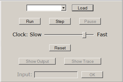
When a program has been loaded, clicking "Run" starts the simulated clock running, and the program runs at a speed proportional to the clock speed. Clicking "Step" executes a single instruction from the location pointed by the program counter. Note that executing a single instruction may take up to six clock cycles.
The "Pause" button stops execution at the end of the current instruction. Because each instruction takes several clock cycles, Pause does not necessarily take effect instantly.
Clock speed: Clock speed is set by a range control (slider.) The speed is variable from a few seconds per pulse to about 50ms. per pulse. Speed changes take effect only at the end of the current instruction, and not immediately.
Reset: The "Reset" button sets the program counter to zero and loads the highest memory location with its own address. Using Reset allows a program to be restarted without re-loading it. Reset is valid only when the clock is stopped.
Show output and show trace: The default is that the green screen area shows the output of the running program. The virtual machine also keeps a record of every instruction that is executed, a trace of the running program. The "Show output" and "Show trace" buttons toggle the output area the program output and program trace. The initial default is to show the output.
Input area: [not yet implemented] The input area is active only when an input instruction is being executed. The clock stops while input is pending and resumes with the input value in the accumulator. Three kinds of input are accepted:
- A decimal number in the range -2,048 to +2,047 The plus sign is not required for non-negative numbers.
- A hexadecimal number, prefixed with "0x" in the range 0x0 to 0xfff. Any value over 0x7ff is interpreted as a negative number in two's complement format.
- A single printable character; the eight bits of the character's ASCII code are stored in the rightmost eight bits of the accumulator.
Register and memory contents: While a program is running on the virtual machine, you can place the mouse cursor over a register or memory cell you see the values in binary or decimal and, for memory cells, how the cell would be interpreted as an instruction. It takes a about a second for the tool-tip to appear.
Breakpoints: Clicking in a memory cell will set a breakpoint at that location. When it is about to be loaded as an instruction, the clock will stop so that you can inspect the contents of memory and registers. Click "Run" or "Step" to continue. Using a memory location as data does not trigger a breakpoint.
Saving the output: Click the "select all" icon on the lower right out the output screen, or click in the output screen and press control-A. Press control-C to copy the selected text to the clipboard; the text may then be pasted into another program such as an editor.
Architecture and Micro-Architecture
TBC is entirely a creature of software emulation, but we wanted to show that it is possible to build hardware that will execute the TBC instruction set. With the exception of input and output, the student who applied himself could, in theory, grundle over to the digital logic lab and build a TBC from logic gates, a clock source, and a power supply. If twelve switches were used for input and twelve LEDs for output, it would be possible to realize all of TBC in hardware using only the information presented here, but you would get only one input operation per program run.
There are some details left out, such as the fan-out of the gates used and the way loading registers from the C-bus on the falling edge of the clock is implemented. These are engineering details, and the fact that they are omitted does not diminish the practicality of the general design.
Early computers and today's simple computers all follow the pattern of registers, an ALU, two input buses and an output bus. The size of the registers and buses and the design of the ALU depend on the instruction set architecture of the computer. The microprogrammed implementation described here is patterned after an implementation described in Andrew Tanenbaum's Structured Computer Organization, Third Edition (1989.)
Memory
The Little Man Computer, after which TBC is patterned, could hold three-digit integers. In two's complement binary, that needs eleven bits, which is a distinctly odd size for a computer word. TBC was designed with a twelve-bit word. That may seem like an odd size as well, but the very successful DEC PDP-8 had twelve-bit words. Data words use twelve-bit two's complement notation, giving TBC an integer range of -2,048 to +2,047. Instruction words have four bits of operation code and eight bits of address. The eight bit address gives TBC a theoretic capacity of 256 words of memory. Like many real computers, TBC is not "maxed out" with memory; only 128 words are "installed" in the simulated computer.
Memory is connected to the CPU by two buses and three control lines. The memory address bus is a unidirectional bus connected to the CPU's memory address register (MAR). The MAR specifies the address in memory to be accessed during a read or write. The memory data bus is a bidirectional bus connected to the memory data register (MDR). The MDR holds data to be written to memory on a write and receives data from memory on a read.
The three control signals are read, write, and presence detect. A read signal commands memory to deliver the contents from the address in the MAR to the memory data bus, and so the the MDR. A write signal commands memory to accept data from the MDR and write it to the location specified by the MAR.
The presence detect (PD) signal causes the memory system indicate the memory size by placing the highest usable memory address on the memory data bus; it will be available at the memory data register (MDR) in the next clock cycle. In a real computer, presence detect returns detailed information about the memory subsystem, including memory size, on a separate serial connection from the memory module. That information is used by the firmware and operating system. TBC uses presence detect to get the address of the stack pointer. In a real computer, the stack pointer is initialized as part of starting a process. Some computers have a stack pointer register to speed up access to the stack pointer.
With the exception of presence detect, memory operations require two clock cycles. Memory timing is discussed below.
Data Path: Registers and Buses
The data path of TBC is shown in Figure 2. The data path of a computer is the arithmetic and logic unit (ALU), the registers, and the buses that connect them. The instruction decoder (I-decoder) / control unit is also shown in the figure. It is discussed in a later section.
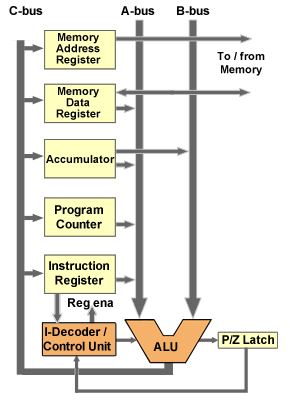
TBC has five registers. The memory address register (MAR) holds one memory address to be used in a memory read or write operation. The MAR is an eight-bit register, allowing TBC to address 256 words of memory. It can be loaded from the C-bus and is connected continuously to the memory subsystem. The memory subsystem only uses this address when commanded to read or write.
The memory data register (MDR) is the same size as the TBC's word size: twelve bits. It can be loaded from the C-bus or driven onto the A-bus. It can also send data to memory on a memory write, or be loaded with data from memory on a memory read.
The accumulator receives the results of arithmetic or logical operations. It is a twelve-bit register. It can drive the A- or B-bus and can be loaded from the C-bus.
The program counter holds the address of the next instruction to be executed. It is an eight bit register that can be loaded from the C-bus and enabled onto the A-bus.
The instruction register holds the instruction currently being executed. It is a twelve-bit register that receives twelve-bit quantities when loaded from the C-bus. When the instruction register is enabled to the A-bus, only the rightmost eight bits are transmitted; the high-order four bits are filled with zeros. The leftmost four bits of the instruction register, corresponding to the operation code of a TBC instruction word, are connected continuously to the I-decoder and control unit.
All three main buses are twelve bits wide. The C-bus can load more than one register simultaneously, although that capability is not used in TBC. Only one register can be enabled to the A-bus and only one to the B-bus during any cycle.
Arithmetic / Logic Unit
The instructions of TBC can be executed with only four ALU functions:
- Add: The addends are enabled on the A- and B-buses; the sum is returned on the C-bus.
- Subtract: The subtrahend (in MDR) is enabled on the A-bus and the minuend (in Acc) is enabled on the B-bus. The difference is returned on the C-bus.
- Copy: The value on the A-bus is copied unchanged to the C-bus.
- Increment: The value on the A-bus is incremented and the new value is returned on the C-bus.
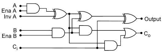
An ALU to compute those functions can be formed from one full adder per bit with three extra gates (two and gates and an exclusive or gate) that provide for control inputs. One bit slice of such an ALU is shown in Figure 3. The Ena A (enable A) control input causes the value on the A bus to be passed to the ALU and adder. The Inv A (invert A) control input causes the value on the A-bus to be inverted before being passed to the full adder. The Ena B (enable B) determines whether the value from the B-bus is passed to the ALU and adder.
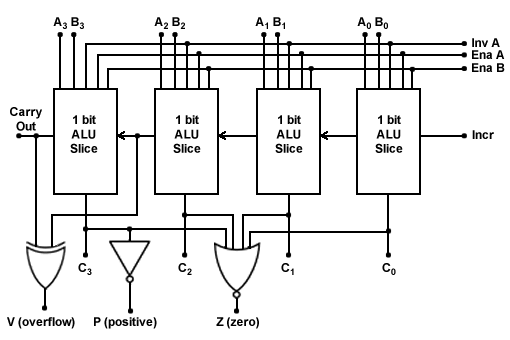
The final ALU is composed of twelve instances of the circuit of Figure 3. A fourth control, increment, is connected to the carry-in bit of the rightmost bit slice. A four-bit configuration of such an ALU is shown in Figure 4.
The four required functions of the ALU are produced with the control signals. In addition, the ALU can emit constants zero, one, and minus one, also shown.
Addition is straightforward; A is enabled, not inverted and B is enabled. For subtraction, the bits of the A-bus, which must be the subtrahend, are inverted by the Inv A control. The Increment control provides for the addition of one to form the two's complement of the value on the A bus, which is added to the minuend on the B-bus. If only A is enabled, the value on the A-bus is copied unchanged to the C-bus. If Enable A and Increment are enabled, the value on the A-bus is incremented (by one) and the result is passed to the C-bus.
If none of the four controls is enabled, the output is constant zero. If only Increment is enabled, the output is constant one. If only Invert A is enabled, the output is all ones, a two's complement minus one.
The V (overflow) signal is asserted when the carry in to the leftmost bit is different from the carry out of the leftmost bit. The P (positive) signal is the inverse of the leftmost bit, which is the sign bit of a two's complement number. So, P is asserted when the value produced by the ALU is non-negative. The Z (zero) signal is asserted when all bits of the ALU result are zero.
P/Z Latch
The arithmetic and logic unit produces a P (positive) signal that is the inverse of the sign bit of the ALU output, so it is a one when the ALU output is non-negative and a zero when the output is negative. It also produces a Z (zero) signal that is the nor of all 12 result bits, and so is a one when the output of the ALU is zero. These signals are input to the P/Z latch. The P/Z Latch is enabled to write concurrently with the accumulator register, so the P and Z outputs always reflect the state of the accumulator contents. The output of the P/Z latch is input to the I-decoder and control unit, providing a mechanism to test the state of the accumulator without requiring an additional data-path cycle.
I-Decoder and Control Unit
TBC's control unit is microprogrammed. The instruction decoder and control unit must generate 17 control signals, as shown in the table. In addition, we need two bits to control branching in the microprogram, one bit to control use of the op code as a branch target, and eight bits of address for jumps. Each microprogram word is 28 bits; for simplicity, we would use a ROM with 32 bit words because these are likely to be commercially available. The layout of the microprogram requires 256 words of ROM, although not all of them are used. The control signals that must be generated are these:
| Data Path Control Signals | ||
|---|---|---|
| ALU | 4 | Enable A (EnaA); Invert A (InvA); Enable B (EnaB); Increment (Inc) |
| Memory | 3 | Read, write, PD |
| A-bus | 4 | Select one of four registers to enable onto the A-bus |
| B-bus | 1 | Indicates that Acc is to be enabled onto B-bus. |
| C-bus | 5 | Selects any of five registers for write from the C-bus |
| Microprogram Controls | ||
| Op Code | 1 | If 1, the operation code from the instruction register, shifted left 4, is used as branch target |
| Jump | 2 | 00=no jump; 01=jump if positive (jp); 10= jump if zero (jz); 11=unconditional jump (ju) |
| Next Addr | 8 | If jump is non-zero, the address of the next microinstruction |
Two of the possibilities for the jump control test the bits pf the P/Z Latch, which reflect the the current contents of the accumulator.
Tanenbaum (1989) described a notation for representing microcode which he called the micro assembly language, or MAL. The two tables below show the add and brp instructions in a notation similar to Tanenbaum's MAL, and with the actual bits of the microprogram. The complete microprogram is here.
| Operation (for add, op code 1 |
Loc | ALU | Mem | Bus control | Op Cd |
Jmp | Next Addr |
||||||||||||||
|---|---|---|---|---|---|---|---|---|---|---|---|---|---|---|---|---|---|---|---|---|---|
| A | B | C | |||||||||||||||||||
EnaA |
InvA |
EnaB |
Inc |
Read |
Write |
PD |
MDR |
Acc |
PC |
IR |
Acc |
MAR |
MDR |
Acc |
PC |
IR |
|||||
| MAR ← PC; rd | 00 | • | • | • | • | ||||||||||||||||
| PC ← PC+1 | 01 | • | • | • | • | ||||||||||||||||
| IR ← MDR; op | 02 | • | • | • | • | ||||||||||||||||
| MAR ← IR[addr]; rd | 10 | • | • | • | |||||||||||||||||
| (wait) | 11 | ||||||||||||||||||||
| Acc ← Acc + MDR; | 12 | • | • | • | • | • | ju | 00 | |||||||||||||
| Operation (for brp, op code 8) |
Loc | ALU | Mem | Bus control | Op Cd |
Jmp | Next Addr |
||||||||||||||
|---|---|---|---|---|---|---|---|---|---|---|---|---|---|---|---|---|---|---|---|---|---|
| A | B | C | |||||||||||||||||||
EnaA |
InvA |
EnaB |
Inc |
Read |
Write |
PD |
MDR |
Acc |
PC |
IR |
Acc |
MAR |
MDR |
Acc |
PC |
IR |
|||||
| MAR ← PC; rd | 00 | • | • | • | • | ||||||||||||||||
| PC ← PC+1 | 01 | • | • | • | • | ||||||||||||||||
| IR ← MDR; op | 02 | • | • | • | • | ||||||||||||||||
| jump positive 82 | 80 | jp | 82 | ||||||||||||||||||
| jump 00 | 81 | ju | 00 | ||||||||||||||||||
| PC ← IR[addr]; |
82 | • | • | • | ju | 00 | |||||||||||||||
Operation code zero (hlt) is handled with digital logic as a special case. A zero in the operation code field is detected using a four-input nor. The output is anded with the Op Code bit of the control word. A result of true stops the processor clock and so stops execution of the microprogram.
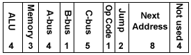
Figure 5 shows the layout of a control word in TBC's microprogram control store. The bits are shown in the order they were discussed above. Tanenbaum (1989) pointed out that they would probably be arranged in a way that minimized crossing of conductors when the CPU was laid out for a semiconductor die. That's an engineering detail that need not concern us while we are working at the level of logical design.
Stack
An extension to the LMC instruction set provides for a stack that grows downward from the highest memory address. The highest memory address is used as a stack pointer. The stack pointer is the address of the first empty stack frame. That allows stack pointer arithmetic to be done after the memory write for a push operation, and so allows pushing the accumulator onto the stack. The stack pointer is initialized with its own location minus one when a program is loaded or the machine is reset. That is, address 0x7F is loaded with the value 0x7E. The call instruction decrements SP and stores the program counter at the location pointed by SP. The ret (return) instruction places the value at location SP into the program counter and increments SP.
The location at the highest memory address can be used for program storage provided the call and ret instructions are not used in such a program and the PD control signal to memory is never asserted.
Timing
The most important thing about understanding timing in TBC (and real computers) is that things do not happen instantly. Computation with digital logic introduces gate delays, and even sending a signal from one part of the CPU to another isn't instantaneous because the signals travel no faster than the speed of light. The purpose of a CPU's clock is to allow enough time for signals to travel through the gates and buses to perform the desired computations. For real computers, clock speeds are measured in gigahertz: billions of pulses per second. For TBC you can adjust the clock speed from a pulse every couple of seconds to several pulses per second. The idea is to make TBC's clock slow enough for you to observe what is happening.
Instruction Timing
The fetch/decode/execute cycle of the Von Neumann architecture means that each instruction consists of some number of individual steps. In TBC, each step is accomplished in one data-path cycle.
Datapath Timing
The datapath of a computer comprises the registers, the ALU, and the buses that connect them. TBC completes one data-path cycle with every cycle of the computer's clock. Each instruction takes multiple data-path cycles, so each data-path cycle does part of the work of one instruction.
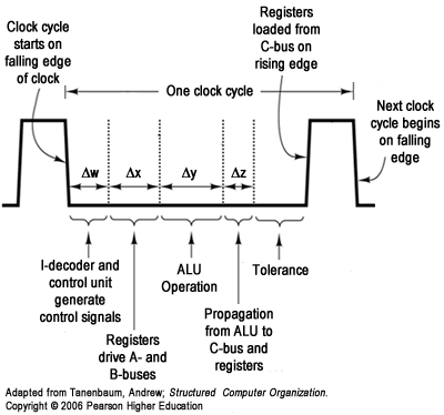
TBC uses an asymmetric clock; that means one part of the cycle, in this case clock-low, is longer than the other part, the clock-high part of the cycle. The clock-low part of the cycle must be long enough for generation of control signals, propagation of data on the buses, and computation by the ALU. By contrast, the clock-high part of the cycle need be only long enough for the registers to be loaded from the C-bus.
A clock cycle starts on the falling edge of the clock. The falling edge triggers the instruction decoder and control unit to set up the necessary signals. That takes a certain amount of time, shown as Δw in Figure 6.
The control signals include register-enable signals for those registers that are to put their contents on the A- and B- buses. The time for the registers to send their contents to the A- and B-buses, and for the signals to reach the ALU is shown as Δx.
The arithmetic-logic unit is combinational logic; it is computing continuously. It's outputs change in response to changes in the inputs. However, the output of the ALU is not valid until it has valid inputs, and for a time after than equal to the gate delay through the ALU. That time is shown as Δy in the figure. It then take time Δz for the output of the ALU to travel along the C-bus and be available at the inputs of the registers.
The last time band in the figure is labeled "Tolerance." Because of manufacturing variation, electronic devices manufactured identically will still be slightly different. The allowance for tolerance means that an instance of this CPU that happens to be slightly slower than the design specification will still work correctly.
By the end of the clock-low portion of the cycle, the result of the current computation has propagated through the C-bus and is available at the inputs of the registers. One or more registers will be selected by the "register enable" signals from the I-decoder and control unit to receive the results, and the results will be stored in those registers on the rising edge of the clock. (Usually a result is stored in only one register, but it is possible to store the same result in more than one.)
Notice that no signals are necessary to trigger operations between the falling edge of the clock and the next rising edge. It is only necessary to hold the clock in the low state for long enough to allow propagation of signals through the buses and the ALU.
Memory Timing
In a real computer, memory is many times slower than the CPU. For a computer with a four GHz clock and 15 ns memory, memory is about 60 times slower; the clock will pulse 60 times before memory delivers a result. To compensate, real computers implement cache memory. Most memory requests can be satisfied from a small, fast cache memory that is only about two to ten times slower than the CPU.
To show that the CPU must often wait on memory, but to keep waiting time from being so long that the simulation is useless, TBC requires two clock cycles for a memory access. That is, if a memory read is commanded in clock cycle one, the result is not available in the memory data register until the beginning of clock cycle three. There must be at least one clock cycle between consecutive writes. Whenever possible, the control unit does useful work while waiting for memory. For example, the program counter is incremented while waiting for memory to deliver an instruction in the "fetch" part of the cycle. Otherwise, the control unit executes a no-operation cycle while waiting on memory.
Input and Output
The in and out instructions are executed "behind the scenes" by the simulator. The out instruction completes in four cycles; the explanation might be that the IO subsystem always has a buffer ready for output and can accept in one clock cycle. The clock is stopped while the in instruction executes. No detail of the I/O process is exposed by the simulator when the LMC I/O instructions are used.
TBC can also do memory-mapped I/O, which exposes programmed I/O with busy waiting to the simulated program. TBC uses the three highest possible memory addresses, 0xfd, 0xfe, and 0xff as registers for I/O. Address 0xfd is the I/O address register, 0xfe is the I/O status register and address 0xff is the I/O data register.
The programmer must store a device address in 0xfd; the input device is 0x000 and the output device is 0x001. For output, the data word to be written must be stored at address 0xff. For input, the value read will be placed in address 0xff. After the registers are set up, the programmer issues the pio instruction. The program must then loop, testing address 0xfe until it becomes one, indicating the completion of the I/O operation. Any input or output operation attempted before 0xfe becomes one will cause a machine check.
References
Tanenbaum, Andrew (1989). Structured Computer Organization, Third Edition. Upper Saddle River, NJ, Prentice-Hall.
Tanenbaum, Andrew (2006). Structured Computer Organization, Fifth Edition. Upper Saddle River, NJ, Prentice-Hall.